What's A Multi-Layered Circuit Board?
Maximum Power In A Minimal Space.
If you've ever opened any electronic device, you've seen a printed circuit board (PCB), which is a collection of electronics that's been laid out in a form that's compact, durable, easy to reproduce, and consistent in performance. Over the last hundred years or so, the techniques for wiring electrical circuitry have got more and more refined, allowing for incredibly complex circuits to be fit into a very small space. How did we get here?
Imagine that we start with just a handful of circuit components that have to be wired together: resistors, capacitors, a transistor or two, maybe a switch. If there aren't too many of them, we could just solder them together directly. To keep the components from rattling around inside the device we're building, we attach them to a piece of non-conductive material — epoxy resin, plastic, or even cardboard — by putting their leads through some holes. Then we flip over the board and solder wires between the proper leads to complete the circuit. This is called 'point-to-point' wiring, and it's still used in vintage-style microphones and certain very simple guitar pedals.
Now, what if our circuit gets more complicated, with a lot of elements to keep track of? Rather than solder a whole lot of wires, we can 'draw' electrical connections (called traces) in a carefully designed pattern on the board, connecting the various holes where we'll solder the components in place. We put all the components where they need to go (called populating or stuffing the board), solder them down, and the circuit's complete because the “wires" are already in place. This is called 'through-hole' design because the components' leads are put through holes before they're soldered.
Sometimes, though, we have components that are so tiny, or have so many connections in such a small space, that we can't drill all the holes we need in the space we have. Instead, we place spots on our traces called pads, where the component's leads or pins simply rest in place and are secured with tiny dots of solder — usually by a machine operating at very high speed. A component that attaches this way is a surface-mounted device (SMD).
Now, what if we have a bunch of through-hole and surface-mounted components, so many that we can't draw all the traces on the front or back of the board without them getting in each other's way? Then we use both front and back, so traces can pass one another without shorting out.
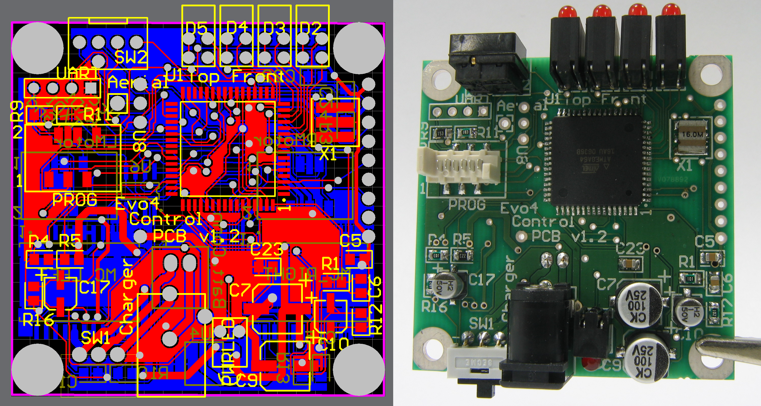
Check out the image below. On the left is a design for a PCB, with outlines for the various components that will populate it (yellow) and traces on the front (red) and back (blue). On the right is the finished device. You can see where there are through-hole connections (grey circles), SMD pads (e.g. the red rectangles around the big square chip), and the many traces connecting them all. Pretty impressive!
This level of density works for circuits with dozens or even hundreds of components… but modern electronics may require thousands of components. Imagine how many circuit boards that would take, and how big the resulting box would be!
To keep these devices' sizes under control, we use multi-layered circuit boards. Imagine a single board with components soldered to both sides, crammed close together. How would we connect them all without a bunch of crossed wires and short circuits?
The easiest way is to have our board as a sandwich of multiple layers, each with its own pattern of traces. Think of the many levels of underground tunnels under a city, where trains can run without hitting each other and only connect where desired. That's the idea behind a multi-layered circuit board.
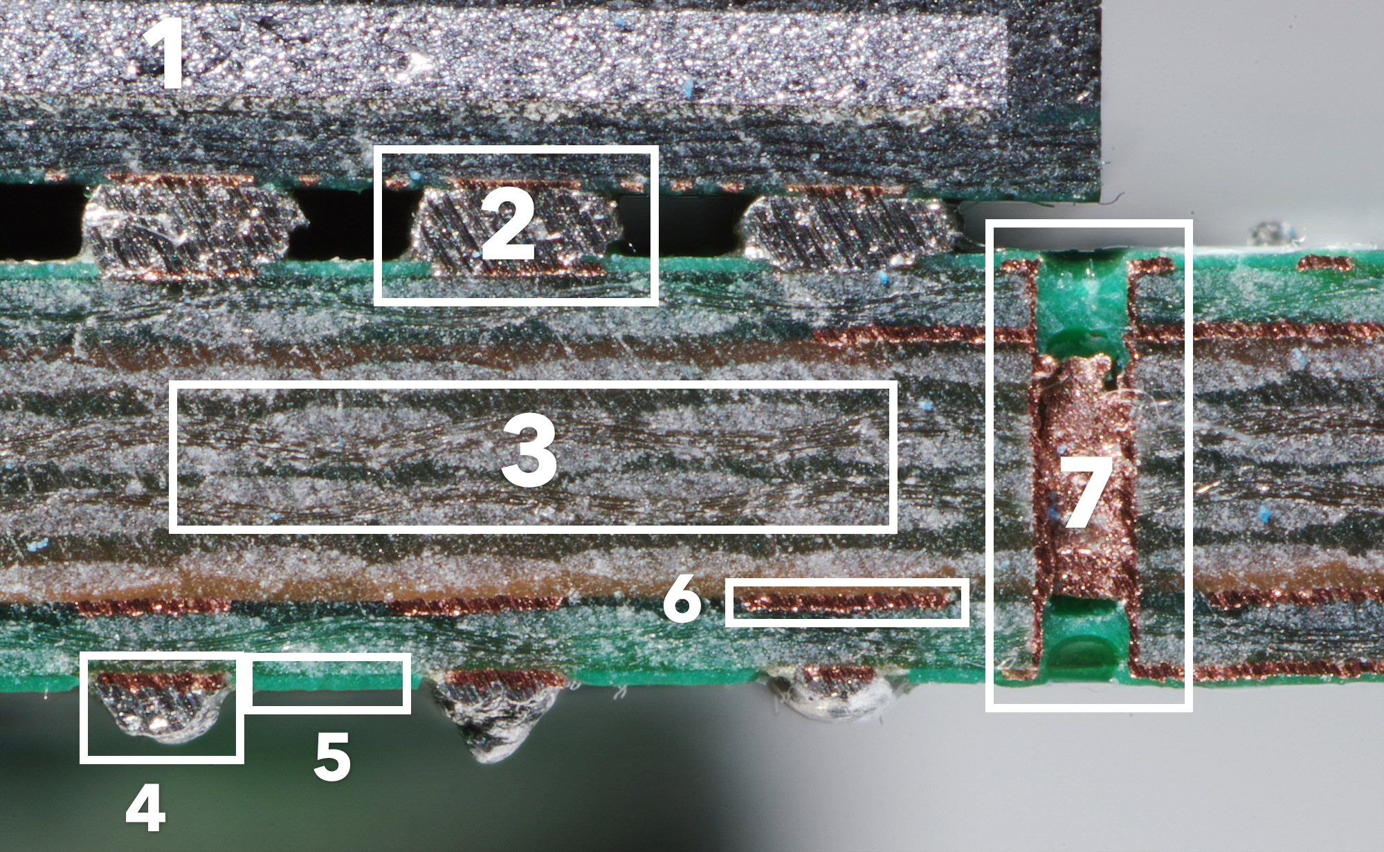
Check out Figure 2 to see an example. This is a microscopic photo of a cross section cut right through an SMD attached to a multi-layered circuit board. The SMD (1) is attached to the top of the board by solder pads (2). The board underneath is made of several layers of glass fiber (3). As you can see, there are the usual external solder joints (4) and the green solder resist that separates them to prevent short circuits (5). Look closer, though, and you'll see other connections inside the board (6), making the overall routing many times more complex without sacrificing quality!
Oh, and how do the different layers connect to each other when they need to? With a special hole called a via (7), which runs a connection up or down between layers like an elevator shaft. Sometimes they go all the way through all the layers, like this one; other times, they may start or stop inside the board and be invisible to the eye.
This multi-layer construction allows for the kind of complexity needed to fit the myriad parts into a single rack space, as you'll find in the Focusrite Red 16Line interface. Offering both DigiLink™ connectors and Thunderbolt™ connections; 16 line inputs and outputs; two main monitor outputs; two Red Evolution mic preamps; world clock I/O and other digital I/O to name just a few features, there's a lot of power in a small box. Now you know how it's done: that it's all thanks to multi-layered circuit board technology.
Words: Diana Smethurt